U.S.-based wafer manufacturer 1366 Technologies has confirmed plans for a 2 GW wafer and cell production facility in India. The unit is being planned under the Indian government’s production-linked incentive (PLI) scheme, which aims to drive deployment of every stage of the solar supply chain, from polysilicon to module manufacturing.
A spokesperson for the company told pv magazine it is exploring manufacturing opportunities for its ‘direct wafer’ production process in India and the business said it is also seeking solar module partners.
“The Indian government has made domestic solar manufacturing a priority and our technology is particularly well suited for the Indian market,” said the 1366 spokesperson. “Direct wafer manufacturing can immediately deliver the lowest cost of electricity in a single-junction device for India’s utility market, and it underpins an economically feasible, high-efficiency, tandem product for global leadership.”
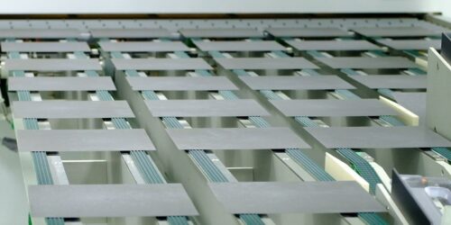
The direct wafer process is a kerfless wafer technique, meaning it does not require silicon ingots to be sawn into wafers, a time-consuming process that wastes material as silicon dust. Instead, 1366’s technology forms wafers directly, using molten silicon. The company claims its direct wafer process offers the world’s lowest wafer production cost, translating into cell and module competitiveness.
The direct wafer approach has long held big hopes for the industry and the company operates a demonstration facility in Bedford, Massachusetts, where most of its technological developments were achieved. One such was a 20.3% cell efficiency level recorded in August 2017 in a Q Cells Q.antum cell which incorporated passivated emitter rear contact (PERC) technology and 1366 wafers. That record, 1366 Tech said at the time, was achieved on a pilot line using standard processes seen in mass production.
This copy was amended on 24/06/21 to reflect 1366 Technologies is planning a wafer and cell facility, rather than just wafers, and that it is seeking solar module, rather than cell partners.


